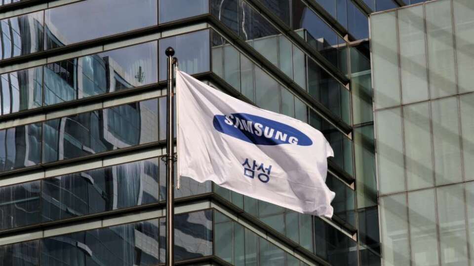
As semiconductor market demand structures shift, Samsung Electronics (005930KS) is accelerating adjustments to its foundry capacity layout. Industry sources indicate that with 4nm process capacity nearing full utilization, Samsung is actively promoting its mature and cost-effective 5nm process to attract domestic and international fabless customers, opening up a new wave of foundry business opportunities.
According to semiconductor industry reports, Samsung Foundry's 4nm process capacity is expected to remain fully loaded into next year. Insiders note that this high utilization rate of the 4nm production line is primarily due to a surge in internal high-bandwidth memory (HBM4) orders from Samsung Electronics itself, elevating its memory division to become the foundry’s largest customer group.
Additionally, NVIDIA's (NVDA-US) inference language processing unit (LPU) 'GROK-3' has exceeded production expectations, further increasing the load on 4nm process capacity.
Facing saturated 4nm production lines, Samsung Foundry is adjusting its strategy by positioning the 5nm process as a key alternative solution.
For fabless customers considering the high costs and yield challenges associated with 2nm or 3nm advanced processes, the already highly mature 5nm process—with its proven high yields and excellent performance—has become the optimal choice balancing efficiency and cost.
Traditionally, the 5nm process was largely seen as a production line dedicated to automotive applications. For example, Hyundai Motors’ planned mass production of advanced driver-assistance systems (ADAS) chips by 2030, Bose Semiconductor’s SoCs, and Telechips’ automotive AP Dolphin 7 chip are all scheduled for mass production using the dedicated automotive SF5A process.
However, as market demands evolve, its application scope has rapidly expanded to include servers, high-performance artificial intelligence, and neural processing unit (NPU) chips.
Another semiconductor industry insider explained that because the 5nm process is also suitable for manufacturing high-performance server chips, licensing agreements with overseas fabless companies continue to be signed. Over the past three to four months, customer demand for the 5nm process has significantly increased.
Furthermore, global geopolitical factors and supply-demand tightness in competitor TSMC’s advanced production lines have indirectly benefited Samsung.
With TSMC experiencing capacity constraints in its 3nm, 4nm, and 5nm processes, fabless companies from China and India are turning their attention to Samsung’s 5nm lines to meet advanced process needs and circumvent related sanctions.
Industry partners point out that for Chinese and Indian customers seeking advanced process performance under U.S. sanctions against China, Samsung Foundry offers a practical solution and has successfully absorbed order volumes from small-to-medium-sized clients displaced by TSMC.
On the other hand, although the 5nm process has become the current core of promotion and actual sales, global customer inquiries and consultations regarding the 2nm process have never ceased.
Industry insiders emphasize that Samsung’s fabrication facilities continue ongoing discussions around the 2nm process, and the key to future breakthroughs lies in ensuring stable mass-production yields.
FACT BOX
- Source: PR Times
- Category: New Product
- Organizations: Telechips
- Products / services: LPU GROK-3