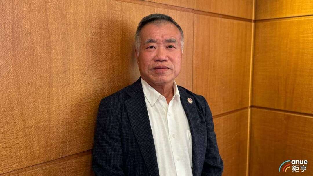
Hong Su (3131-TW) today announced that its subsidiary, Jia Lin Technology, has partnered with Japan’s Seikyo Semiconductor Co., Ltd. to officially represent the company’s full lineup of advanced bonding and precision surface treatment equipment in Taiwan. This collaboration combines Japanese core technology with Hong Su’s equipment manufacturing, wet process, engineering integration, and supply chain capabilities in Taiwan, driving the localization of key equipment and process technologies.
Hong Su noted that AI and HPC continue to drive demand for advanced packaging. As chip stacking, heterogeneous integration, and backside power delivery technologies rapidly evolve, bonding technology has become a critical process in the next phase of advanced packaging.
Hong Su emphasized that this partnership is more than just equipment distribution—it marks a strategic step for the group to establish a foothold in key advanced packaging processes and deepen Taiwan’s bonding equipment manufacturing capabilities. Taiwan already possesses a robust foundation in advanced packaging manufacturing and supply chains, gradually building self-reliance in processes such as cleaning, bonding, molding, and dispensing. However, there remains significant reliance on overseas suppliers for high-end chip stacking and hybrid bonding (Hybrid Bonding) equipment. Through this partnership, Jia Lin will begin with product distribution and local services, leveraging Hong Su’s existing manufacturing and supply chain strengths to gradually build a more comprehensive equipment and process service capability.
One of Seikyo Semiconductor’s core technologies is Surface Activated Bonding (SAB), derived from long-term research by Professor Yuzuru Suga of the University of Tokyo. Compared to traditional bonding methods, SAB uses surface activation and bonding in a vacuum environment, enabling materials to bond under highly clean and activated conditions. This allows high-quality bonding at low temperatures, even near room temperature, reducing thermal stress caused by differences in thermal expansion coefficients between materials.
SAB’s applications extend beyond wafer-to-wafer (W2W) and heterogeneous material bonding, with potential expansion into emerging areas such as high-efficiency heat dissipation, backside power delivery, and integration of high-thermal-conductivity materials. As AI chip computing density and power consumption continue to rise, simultaneously addressing computing power, thermal management, and energy efficiency has become a key challenge in advanced packaging development. SAB’s low-temperature bonding and heterogeneous material integration capabilities offer significant potential for future high-performance thermal management and novel material integration applications.
Professor Yuzuru Suga, technology advisor at Seikyo Semiconductor, stated that the key to heterogeneous integration lies in precise control of the cleanliness, flatness, and surface activation state of the bonding interface. SAB enables high-strength bonding at low or near-room temperatures, helping to reduce stress from thermal expansion differences between materials. By further integrating with Hong Su’s wet cleaning and surface treatment capabilities, there is potential to establish a complete technical platform from pre-bonding surface preparation to precision bonding.
In addition to SAB, Seikyo Semiconductor is also developing hybrid bonding and Fast Super-Atom Beam (FSB) surface treatment technology. Prior to hybrid bonding, highly precise cleaning, planarization, and surface treatment of wafers or chips are performed, followed by precision bonding of dielectric materials and metal interfaces. This supports architectures such as W2W and Chip-to-Wafer (C2W), and can be applied to advanced packaging technologies including 2.5D IC, 3D IC, Chiplet, and backside power delivery.
The surface condition prior to bonding is a critical factor determining yield and reliability in advanced packaging. Seikyo’s FSB precision surface treatment technology further controls wafer surface roughness within bonding-suitable ranges, forming an interconnected technical capability with SAB and Hybrid Bonding, thereby strengthening process integration for high-end chip and wafer stacking.
Hong Su Chairman and CEO Zhang Hongtai stated that Taiwan has already established a complete manufacturing foundation for advanced packaging. However, to further master next-generation chip stacking and heterogeneous integration technologies, high-precision bonding and advanced surface treatment are indispensable components. Through this partnership between Jia Lin and Seikyo Semiconductor, the goal is to bring mature Japanese bonding technologies into Taiwan and, by combining them with Hong Su’s existing wet process, equipment manufacturing, and supply chain capabilities, gradually build localized capabilities from surface treatment and activation to bonding and process verification.
Seikyo Semiconductor’s General Manager Ye Guoguang stated that Seikyo hopes to leverage Jia Lin’s local service capabilities to accelerate the introduction of Hybrid Bonding, SAB, and FSB precision surface treatment equipment into the Taiwan market. At the same time, by integrating with Hong Su’s wet process technology, the two companies aim to jointly develop integrated solutions that meet customers’ mass production needs, accelerating the verification and application of technologies such as 3D IC, Chiplet, silicon photonics, and heterogeneous material bonding.
The first phase of cooperation will see Jia Lin Technology serve as the sales and service window for Seikyo Semiconductor’s products in Taiwan, gradually establishing capabilities in equipment sales, application engineering, process verification, custom integration, and after-sales service. On this foundation, both parties will continue to explore deeper and more diverse collaboration possibilities through technology exchange, resource integration, equipment manufacturing, application development, and market expansion, further deepening cooperation in the field of advanced packaging.
Hong Su stated that from 2.5D IC, 3D IC, and Chiplet to backside power delivery, Taiwan’s semiconductor industry is transitioning from traditional planar scaling processes toward chip stacking and heterogeneous integration. This partnership with Seikyo Semiconductor, based on core technologies such as SAB, Hybrid Bonding, and FSB precision surface treatment, combined with Hong Su’s Taiwan manufacturing and supply chain capabilities, will gradually promote the localization of key equipment and processes, filling a critical technological gap in Taiwan’s advanced packaging and positioning for growth opportunities in next-generation semiconductor advanced packaging.
FACT BOX
- Source: PR Times
- Category: Partnership