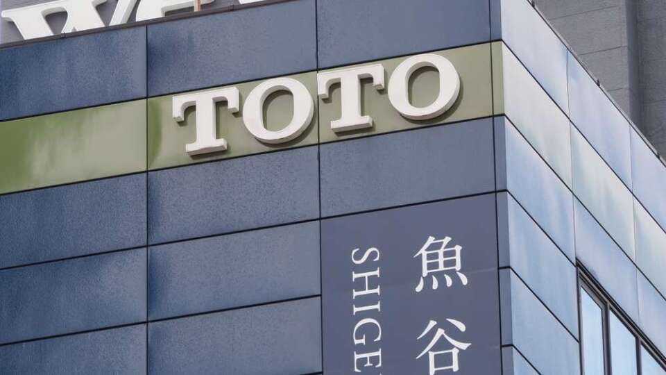
TOTO, globally recognized for its toilets and sanitary equipment, is formally entering the AI semiconductor market. In response to surging demand for AI GPUs, HBM, and advanced chips, TOTO has announced a 300 billion yen investment to expand its advanced ceramics business for semiconductors. Of this amount, 170 billion yen will be allocated to constructing a new ceramic research building at its Chigasaki site, transforming decades of accumulated ceramic technology into a new growth engine.
TOTO’s involvement in precision ceramics is not a recent development. The company began research in 1976 and formally launched its ceramic business in 1984. Under its medium- to long-term strategy 'WILL2030,' TOTO has positioned advanced semiconductor ceramics as a core growth area, expanding its business scope from traditional sanitary ware to semiconductor and optical communication markets.
Currently, TOTO’s semiconductor ceramic products include electrostatic chucks (ESC) and AD (Aerosol Deposition) ceramic components. Electrostatic chucks use electrostatic force to secure wafers and are critical components in semiconductor manufacturing equipment, especially in advanced processes where temperature control, flatness, and particle management are extremely stringent.
The AD aerosol deposition technology involves spraying ceramic powder at near-sonic speeds to form dense yttria (Y2O3) ceramic films. These films exhibit strong resistance to plasma corrosion, reducing particle contamination during chip production and outperforming traditional thermal spray processes.
With the explosive demand for AI GPUs, HBM, and advanced chips, the need for these ceramic components continues to grow.
Expanding R&D and Mass Production Simultaneously
To capture semiconductor demand, TOTO is expanding both R&D and manufacturing. R&D will be centered at the Chigasaki site, where the new research building will focus on next-generation ESC and AD component technologies. Mass production will be handled at the Nakatsu and Buzen factories.
Notably, construction of the ESC sintering facility at the Buzen plant began in December 2025, with operations scheduled to start in January 2027. The Nakatsu plant has also completed multiple rounds of expansion, enhancing production capacity. Through this 'Chigasaki for R&D, Nakatsu and Buzen for manufacturing' division of labor, TOTO is gradually establishing an integrated system covering material development, design, production, and performance verification.
AI Demand Propagates Upstream to Materials
The demand driven by AI computing power expansion is no longer limited to GPUs and HBM but is now extending to semiconductor equipment and materials. Components once considered niche, such as electrostatic chucks and yttria coatings, have become essential in high-temperature, high-plasma wafer processing environments, where the quality of high-performance specialty ceramics directly impacts process yield.
TOTO is transferring its long-standing material and sintering expertise from the sanitary ceramics field to semiconductor materials. This investment is not the final phase—TOTO plans further large-scale production expansions. As AI semiconductor demand reaches upstream materials, traditional ceramic manufacturers are increasingly integrating into the semiconductor supply chain.
FACT BOX
- Source: PR Times
- Category: New Product