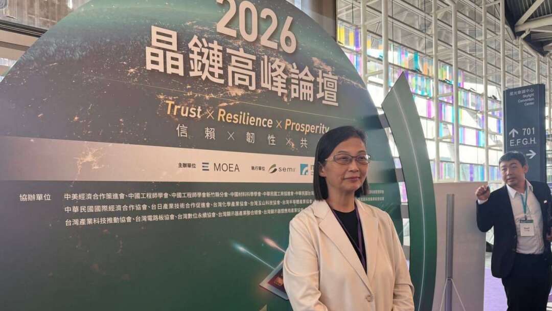
Hsu Hsiu-Lan, Chairman of GlobalWafers (6488-TW), a leading silicon wafer manufacturer, stated today (1st) that AI is driving structural changes in semiconductor demand, leading to continuously increasing needs for silicon wafers. She expects the silicon wafer industry to have a strong chance of maintaining double-digit growth over the next two years, with both price and volume rising—a scenario she described as 'price-volume expansion.' Long-term contract pricing is still under negotiation with customers, though some agreements are nearing completion, hinting that the 'direction is quite healthy.'
Hsu attended the 2026 JingLian Summit Forum today, where she was awarded the 'Ministry of Economic Affairs Professional Award.' In a post-event interview, she noted that as technology evolves, wafers are becoming increasingly complex and specialized. Beyond traditional silicon wafers, square wafers, wafers of various shapes, and compound semiconductors are now emerging. Wafers themselves have evolved from being opaque in the past to now including many transparent variants, changing even measurement methods. 'Today’s wafers are more complex, more interesting, and more challenging than they’ve been in the past 60 years,' she said.
Hsu expressed optimism that, as customers continue large-scale factory expansions, even before new plants are completed, existing facilities are also ramping up capacity to shorten time-to-market and accelerate shipment volumes. She believes double-digit growth in silicon wafer industry output value over the next two years is highly achievable, with both shipment volumes and sales prices expected to improve.
Regarding advanced packaging, Hsu pointed out that a wide variety of wafers are involved, including square wafers, larger silicon carbide (SiC) wafers, fully transparent SiC wafers, and various thermal dissipation materials. While GlobalWafers’ revenue from advanced packaging was very small last year, this year has already seen part of its revenue coming from this segment, and she holds strong positive expectations for future growth in this area.
On CPO (Co-Packaged Optics) initiatives, Hsu stated that GlobalWafers is most active in the field of silicon photonics, particularly focusing on using 12-inch silicon wafers as waveguide substrates. The company plays multiple roles in this domain, including developing waveguides for different wavelength bands, which are current key focus areas.
GlobalWafers currently possesses materials such as silicon wafers, silicon carbide, and gallium nitride, and is also exploring new material solutions. Since some future CPO products may require wafer materials that are harder to obtain and currently in short supply, GlobalWafers is actively catching up, though it remains in the R&D phase for now.
FACT BOX
- Source: PR Times
- Category: Event