As artificial intelligence (AI) chip computational power continues to rise, the shift toward 3D structures, heterogeneous integration, and system-in-package designs has made data transmission power consumption, die interconnect density, and advanced packaging yields new technological bottlenecks. Applied Materials (NASDAQ: AMAT) will focus on fine-pitch hybrid bonding, die-to-wafer (D2W) integration, and panel-level packaging (PLP) at SEMICON Taiwan 2026, introducing digital lithography and agentic AI to break through energy and mass production limits for AI chips—from materials, interconnects, patterning, and smart manufacturing.
AI is transforming semiconductor innovation models. In the past, chip performance improvements relied heavily on transistor scaling. However, as advanced process technologies become increasingly complex and costly, the industry is turning to chiplets, 3D stacking, and heterogeneous integration—integrating dies of different processes and functions into a single system to boost computing performance.
This shift has elevated packaging from a back-end step after chip fabrication to a critical technology directly impacting system performance, power consumption, and yield. The synchronized development of materials, processes, equipment, and packaging will determine how quickly new technologies move from R&D to mass production.
Yu Ting-Lu, Group Vice President of Applied Materials and President of Taiwan Applied Materials, stated, "AI is increasing the complexity of semiconductor innovation, and every breakthrough depends on collaborative innovation across the ecosystem." With 36 years of presence in Taiwan, Applied Materials will continue collaborating with customers, partners, and the supply chain, leveraging its materials engineering and interconnect product portfolio to accelerate the transition from R&D to volume manufacturing.
Hybrid Bonding Enhances Interconnect Density and Reduces Power Consumption
As AI chips adopt 3D stacking and heterogeneous integration, shortening data transmission distances between dies has become crucial for lowering power consumption. Ashok Kumar Muthukumaran, Senior Director at Applied Materials, will present the latest developments in fine-pitch hybrid bonding and die-to-wafer (D2W) integration at the Semiconductor Advanced Process Technology Forum.
Hybrid bonding establishes ultra-fine interconnects between dies or wafers, enabling higher interconnect density compared to traditional bump bonding. This reduces the data transmission distance between compute dies and memory components. As AI processors integrate more dies, this technology promises to accommodate more interconnects within limited package areas while lowering power consumption from data movement.
Die-to-wafer integration allows dies of different functions, sizes, and even different process nodes to be integrated onto a single wafer platform, enabling flexible combinations of AI processors, memory, and other functional components based on system requirements. Applied Materials believes that higher interconnect density, lower power consumption, and scalable heterogeneous integration architectures can help the industry overcome energy bottlenecks in AI computing.
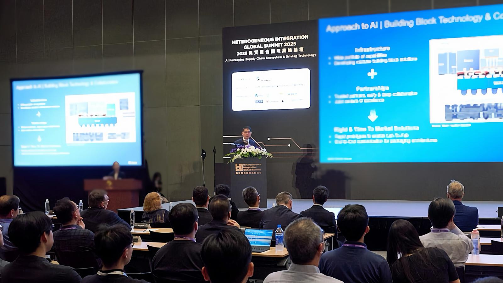
Senior Technical Director Chang-Yi Lan will also chair the Heterogeneous Integration International Summit, focusing on "AI Packaging Supply Chain Ecosystem & Driving Technology," to discuss the AI advanced packaging supply chain and key enabling technologies.
Larger Panel Sizes Bring Greater Challenges in Patterning Precision and Yield
In addition to hybrid bonding, panel-level packaging (PLP) is another key focus for Applied Materials at SEMICON.
Compared to traditional wafer-based packaging, PLP uses larger rectangular substrates to process multiple packages simultaneously, improving area utilization and production efficiency. However, as manufacturing platforms grow larger, issues such as plating uniformity, panel warpage, pattern misalignment, and exposure accuracy become more pronounced, making yield control a critical challenge for PLP commercialization.
Michael Rosshirt, Customer Technical Director at Applied Materials, will introduce the company’s PLP product portfolio, including panel-level electrochemical deposition (ECD) technology, which helps manufacturers build the metal interconnect structures required for advanced packaging on larger panel platforms.
On patterning processes, Anant Chimmalgi, General Manager of Applied Materials’ Digital Lithography Business Group, will present maskless digital lithography and digital dynamic linking. These technologies enable real-time correction of exposure deviations based on actual panel position and deformation, improving patterning accuracy and process yield for large panels.
Unlike traditional fixed-mask exposure, digital lithography adjusts patterns digitally, adapting to positional shifts during panel processing. As advanced packaging linewidths shrink and panel sizes expand, real-time correction capability becomes essential for accurate interconnect alignment.
Agentic AI Enters Fabs: From Automation to Autonomy
Applied Materials is extending AI applications from the chip side to manufacturing sites. Mingyuan Zhao, Senior Strategic Marketing Manager of the Automation Products Business Group, will explain how agentic AI can drive semiconductor fabs from automated production toward autonomous operations at the High-Tech Smart Manufacturing Forum.
While fabs already use extensive automation and manufacturing execution systems, engineers still need to manually review data, compare process parameters, and diagnose root causes when anomalies occur. Applied Materials’ AI-driven system aims to detect anomalies in real time, perform root cause analysis, and support decision-making—reducing troubleshooting time and improving yield, productivity, and operational resilience.
Applied Materials will participate in SEMICON Taiwan 2026 technical forums from August 31 to September 4, 2026. Its focus on hybrid bonding, panel-level packaging, and agentic AI reflects a broader shift in AI chip competition—from a race solely on process node scaling to a system integration battle across materials, equipment, packaging, and smart manufacturing. Balancing high computing power with controlled power consumption, while maintaining mass-producible yields and costs, will define the next phase of semiconductor industry competition.
FACT BOX
- Source: PR Times
- Category: Event
- Organizations: Applied Materials