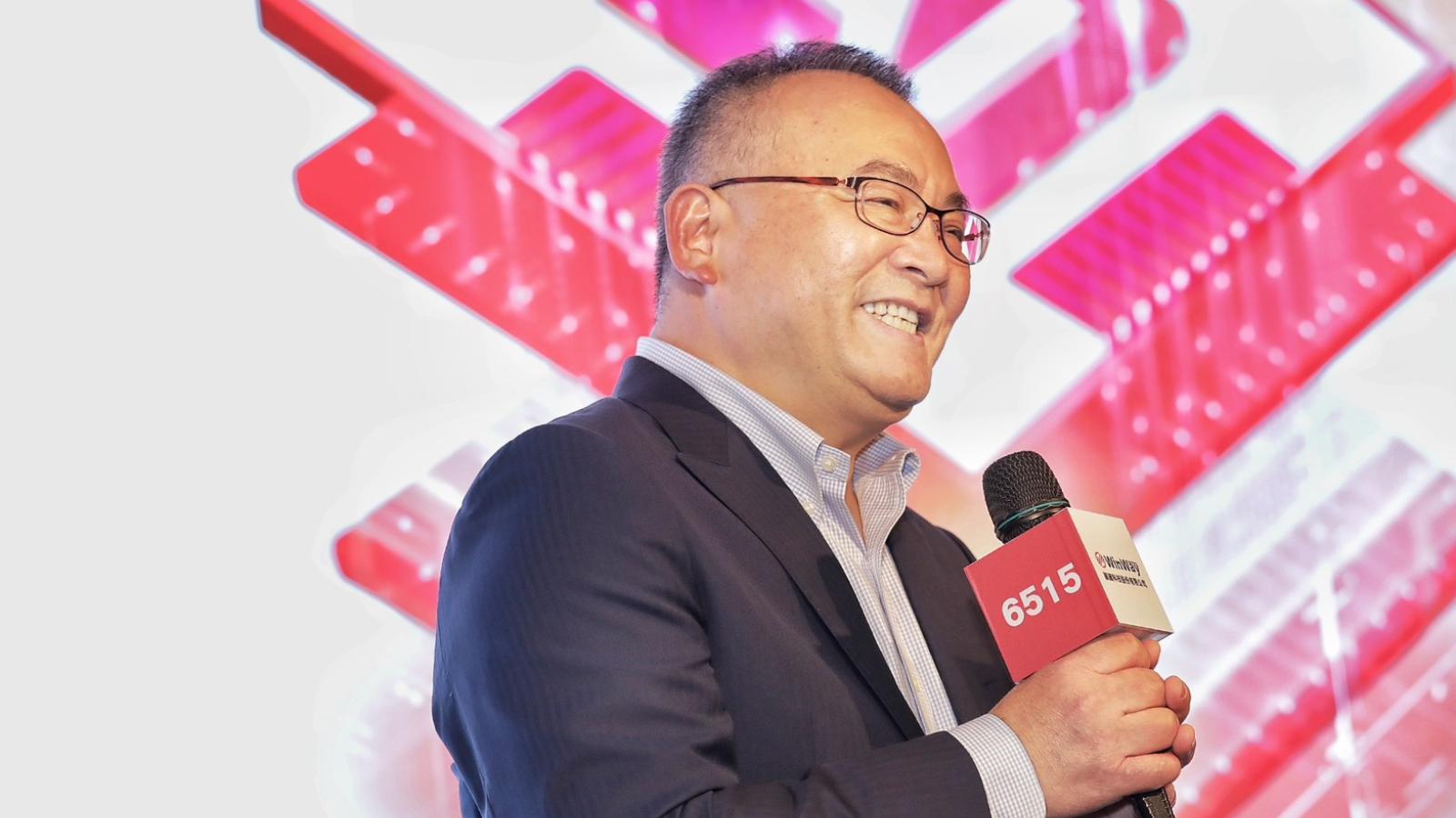
Co-Packaged Optics (CPO) is gradually transitioning from technical validation to commercialization, with test interfaces becoming a critical factor for scalable mass production. Chen Shao-Kun, Executive Deputy General Manager of Winson's Global Business Operations Center, revealed on the 2nd that the company currently holds over ten CPO-related projects, covering major global clients. In CPO socket-related projects, over 90% adopt Winson's test solutions. He estimates that CPO will begin small-volume production as early as the second half of 2027, with more significant mass production likely not occurring until 2028.
However, moving CPO from 'being able to make it' to stable mass production still faces challenges in optical alignment, precision, speed, and automation. Chen frankly stated, 'The industry can now produce CPO products, but the biggest challenge is how to achieve scale and mass production.'
Starting in 2019: Testing Evolves from Electrical Signals to Optoelectronic Integration
Chen noted that Winson began proposing CPO testing concepts in 2019, making it one of the earlier domestic companies to invest in related technologies. At that time, market discussions on CPO were not widespread, and related technologies, equipment, and materials were not fully ready. It wasn't until recent years, with the rapid rise in AI computing power and high-speed transmission demands, that silicon photonics and CPO gradually moved toward practical applications.
Testing technology has also evolved. Traditional semiconductor testing primarily handles electrical signals, but with silicon photonics and CPO, it must not only process optical signals but also integrate optical and electrical testing systems, increasing the complexity of alignment, signal transmission, and test interfaces.
'In the past, we started with electricity, then added light; now, both optical and electrical elements must be integrated,' said Chen. CPO spans a broad range, from fiber array units (FAU), lasers, packaging to mass testing, each stage presenting different technical challenges. Therefore, Winson does not span all domains but continues to focus on its core testing business.
From Wafer Level to Module Level: Insertion 3 and 4 Enter via Socket
In CPO testing deployment, Winson has established corresponding solutions for different manufacturing processes and assembly stages. Chen pointed out that Insertion 2 primarily corresponds to Wafer/Chip Level testing. Winson has developed solutions in MEMS, Wafer Level CPO, and Double-sided Probing, with related prototype equipment undergoing continuous validation at customer sites.
Insertion 3 moves into post-packaging testing, while Insertion 4 further corresponds to larger Module Level testing. Winson is currently allocating more resources to Insertion 3 and 4, primarily entering through Socket test solutions, while also continuously building wafer-level probe cards and optoelectronic testing technologies.
Chen stated that, after re-evaluating company projects before the interview, there are currently over ten CPO-related initiatives, covering nearly all major global clients. 'In the entire CPO socket segment, we won't claim 100%, but over 90% use our solutions for testing.'
However, this percentage refers mainly to CPO socket and module-level projects that Winson is involved in, not the global market share across all equipment, components, and testing segments in the entire CPO industry.
Being Able to Make It ≠ Able to Mass Produce: Automation Bottlenecked by Precision and Speed
Although CPO-related products are gradually entering validation, Chen believes the current biggest bottleneck remains automation.
CPO testing involves fiber and component alignment, different wavelengths, optical precision, electrical signals, and temperature control. If many processes still rely on manual operations, it is difficult to increase testing speed and maintain consistency in mass production.
He summarizes CPO mass production requirements into two key factors: precision and speed. First, optical testing alignment tolerances are extremely small, with different wavelengths and component positions affecting results. Second, if alignment and testing processes cannot be automated, testing speed cannot be improved, and production costs cannot be effectively reduced.
'The biggest problem now is that you can make the product, but how do you achieve scale and mass production?' Chen emphasized that the next stage of CPO is no longer about whether a single product can pass functional validation, but whether a repeatable, stable, and efficient mass production process can be established.
Small Volume from Late 2027, Clear Scale by 2028
Regarding the CPO industry timeline, Chen views 2025 as the 'Year One' of CPO, with 2026 entering a phase of gradually establishing equipment, architecture, and supply chains. If automation, optical alignment, and related mass production support progress smoothly, small-volume products may begin appearing in the second half of 2027. However, a more noticeable market scale may still have to wait until 2028.
To establish mass production capabilities early, Winson is also seeking domestic and international partners, including laser and other optical technology companies, aiming to complement the technologies required for testing systems and accelerate optoelectronic integration and automation.
Chen emphasized that semiconductors are a highly globalized industry. Although Taiwan has a complete manufacturing ecosystem, it must remain open and introduce appropriate technologies, materials, and equipment to push CPO from individual technological breakthroughs to mass production.
AI Chips Must Simultaneously Solve 'Power, Heat, Data' Triad
The fundamental reason for rising CPO demand is the increasing data transmission pressure on AI chips. Chen stated that AI large packaging can be simplified into three problems: 'Power must come in, heat must dissipate, and data must go out.'
As chip power consumption increases, power delivery and heat dissipation have become critical bottlenecks for AI servers. Meanwhile, traditional copper interconnects are increasingly facing bandwidth, power consumption, and transmission distance limitations. Even if chips have higher computing power, if data cannot be effectively transmitted, system performance cannot be fully utilized, driving the industry to accelerate the adoption of optical transmission and CPO.
However, integrating optical signals into packaging also makes testing more complex. Test interfaces must not only handle high-frequency, high-speed electrical signals but also simultaneously manage optical signal alignment, thermal management, and mechanical deformation caused by large packaging.
AI Chip Pin Count Approaching 20,000, Test Pressure Reduced to 30 PSI
Large packaging and high pin count also make warpage a new challenge in testing. Chen pointed out that past CPUs had about 5,000 to 6,000 pins, while current AI chips have increased to about 10,000 pins, some reaching 13,000 pins, with the next generation potentially approaching 20,000 pins.
The larger the package size, the more pronounced warpage typically becomes. In the past, about 70 PSI pressure could be applied during testing to flatten the package and ensure proper contact at each point. However, as chip structures become more complex, customer limits on acceptable pressure continue to decrease, with some requiring reductions to 50 PSI, or even only tolerating 30 PSI.
'You can't press that hard, yet you need warped products to be tested normally—this becomes a critical issue,' said Chen. Warpage levels vary across different chips and packages, so test interfaces must be adjusted for individual products, no longer relying on a single standard structure.
He stated that Winson's current HyperSocket supports products within 20,000 pins, estimated to meet AI chip demands for the next two years, and can improve contact, heat dissipation, and warpage issues caused by large packages. However, as package size and power consumption continue to rise, next-generation products will still need to introduce new thermal architectures.
Liquid Socket Brings Fluid into Socket, Directly Removing Bottom Heat
In addition to top-side heat dissipation, the contact area between the chip and substrate is also a significant heat source. Chen pointed out that when chips operate at high frequency and speed, the bottom contact points also generate substantial heat. Therefore, in the future, it won't be sufficient to rely only on top-side heat sinks; bottom-side packaging heat must also be managed.
To meet next-generation high-power chip demands, Winson has planned to integrate Liquid Socket into the HyperSocket architecture, allowing fluid to enter the socket interior and directly remove heat generated at the chip-substrate contact area.
Related products are already in preliminary cooperation with major global IC design customers and are expected to enter market validation soon. Chen stated that Liquid Socket may not be a universal requirement for this generation of chips, but as chip power consumption, pin count, and package size continue to increase, the need for bottom-side heat dissipation in next-generation products will become clearer.
With over ten CPO projects, socket solution adoption exceeding 90%, and a timeline projecting small volume in late 2027 and mass production in 2028, Winson has secured an early market position. However, whether CPO can truly enter a large-scale market still depends on whether optical alignment, automation, heat dissipation, and supply chain integration can simultaneously overcome mass production thresholds.
FACT BOX
- Source: PR Times
- Category: New Product
- Products / services: HyperSocket / Liquid Socket