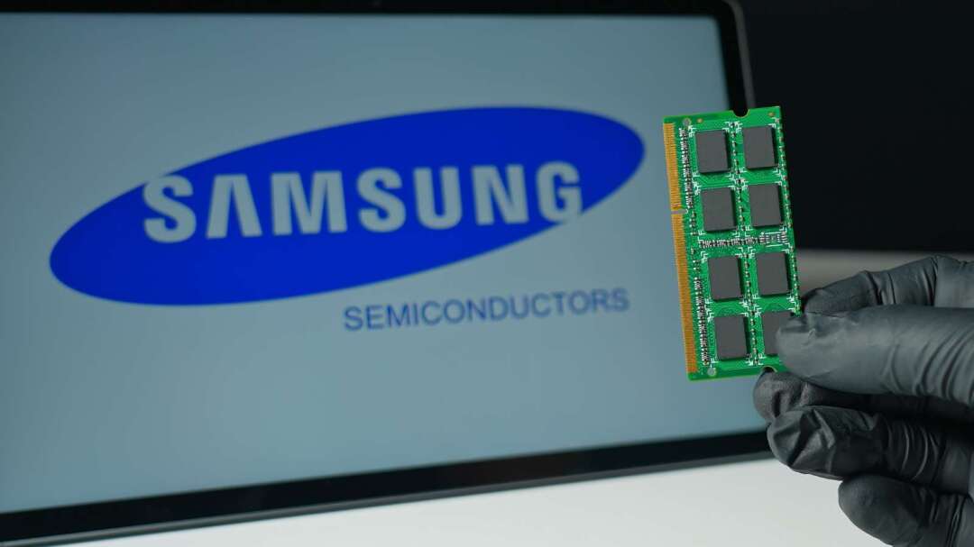
Samsung Electronics unveiled two concept products, zHBM and zNAND-O, along with the industry's first stacked-over-400-layer V10 BV-NAND at the FMS summit in Santa Clara, USA. This bold move positions Samsung to directly challenge SK Hynix and Micron in its bid to reclaim leadership in the memory market during the AI era.
The most anticipated product is zHBM, which completely redefines the current 2.5D packaging architecture. Instead of placing HBM and AI chips side-by-side on a silicon interposer, zHBM vertically stacks the memory directly on top of the accelerator.
At FMS, Samsung claimed that by leveraging wafer bonding technology to drastically shorten data paths, zHBM can achieve up to 8x the performance of the next-generation HBM5, over 10x memory density, 3x better energy efficiency, and over 50% lower thermal resistance. It also supports custom IP integration and is scheduled for mass production in 2029.
Simultaneously, Samsung revealed it had already mass-produced HBM4 in February using its 1c DRAM process and 4nm base die—the first in the world—and delivered HBM4E samples to customers in May.
For edge AI applications, Samsung introduced zNAND-O, differentiating it from SK Hynix and SanDisk’s jointly announced HBF. While HBF targets server-side to bridge the gap between HBM and SSD, zNAND-O focuses on on-device large model storage. Utilizing TSV and UCIe interfaces, it delivers high space efficiency, low latency, and high I/O performance, with mass production expected in 2028.
Regarding V10 BV-NAND, 13 years after the debut of the original V-NAND in 2013, Samsung introduced wafer bonding architecture for the first time, stacking over 400 layers. This results in a 58% increase in storage density compared to V9 and comprehensive optimization of read/write and I/O performance, providing high-density NAND support for AI systems.
Samsung also showcased its full-stack strategy: LPDDR5X-PIM is the industry’s first in-memory computing LPDDR memory; enterprise-grade PM1763 and BM1773 target AI data center memory demands.
As the world’s only IDM that simultaneously controls memory, foundry, and advanced packaging, Samsung aims to shorten customer development cycles with one-stop solutions, widening its lead in the AI infrastructure race. The market will closely watch whether these 'visionary' technologies can be realized on schedule and translate into tangible market share.
FACT BOX
- Source: PR Times
- Category: New Product
- Products / services: zHBM / zNAND-O