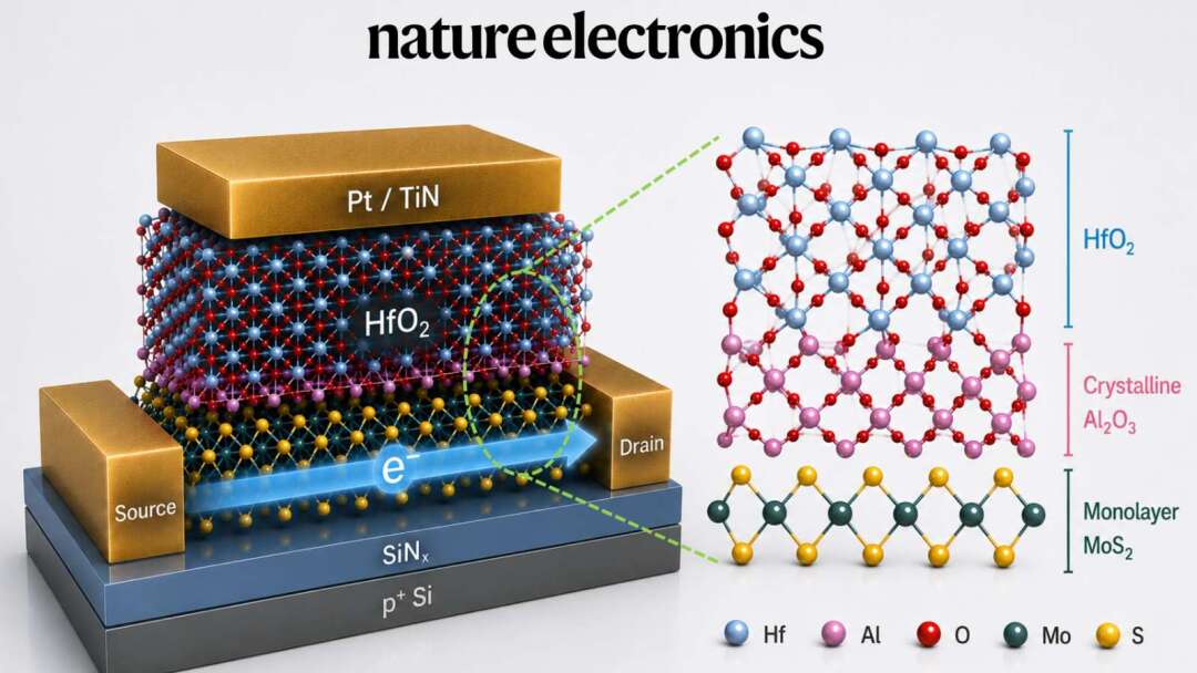
With support from the National Science and Technology Council (NRC) program, Professor Zhang Wenhao’s team from the Department of Electrophysics at National Yang Ming Chiao Tung University (NYCU) and the Applied Science Research Center at Academia Sinica joined forces with Dr. Iuliana Radu’s team at Taiwan Semiconductor Manufacturing Company (TSMC; 2330-TW) and Professor Li Tsung-En from NYCU’s Department of Semiconductor Engineering. Together, they have addressed the persistent 'interface challenge' faced by two-dimensional (2D) semiconductors. Today (6th), they announced the successful development of a high-performance top-gate transistor using monolayer molybdenum disulfide (MoS₂), a breakthrough achievement now featured in the international premier journal Nature Electronics.
Devices ranging from smartphones and computers to future AI-powered smart systems demand semiconductor chips with faster processing speeds and lower power consumption. However, conventional silicon-based semiconductor technology is gradually approaching its physical limits. To overcome this barrier, scientists worldwide are actively searching for next-generation semiconductor materials. Among these, '2D semiconductors'—materials as thin as a single atom—are widely regarded as a crucial enabler for extending Moore’s Law and continuing the miniaturization and performance enhancement of chips.
The research team notes that while 2D semiconductors offer the advantage of ultimate thinness, their practical implementation in chips faces a critical hurdle: a super-thin 'gate dielectric layer' must be deposited to control electrical current. Achieving both an ultra-thin structure and high-speed electron transport has remained a formidable challenge for the global semiconductor community. The innovation by Taiwan’s industry-academia-research team lies in re-engineering the structure of this 'film' using 'epitaxial interface engineering'.
Employing ultra-high vacuum technology, the team first precisely deposited an ultra-thin aluminum layer onto the surface of monolayer MoS₂. This was then oxidized to form an aluminum oxide layer approximately 0.42 nanometers thick, serving as a high-quality substrate for subsequent material growth. This approach significantly improved the interface quality between the 2D semiconductor and the dielectric layer while effectively reducing electron transport resistance. As a result, the team successfully achieved both 'ultra-thinness' and 'high transconductance'—two critical characteristics. The fabricated transistor demonstrated world-leading transconductance performance at extremely small dimensions, along with exceptionally low leakage current and excellent operational stability, showcasing the significant potential of 2D semiconductor devices for real-world applications.
Professor Zhang Wenhao stated that the true competition in 2D semiconductors will no longer be about the materials themselves, but rather about interface engineering. The greatest value of this technology lies in establishing a versatile platform applicable to various 2D semiconductor materials. In the future, this could enable the development of faster, lower-power electronic components that seamlessly integrate with existing semiconductor manufacturing processes, laying a vital foundation for chip technologies in the 'post-silicon era.' This achievement reaffirms Taiwan’s innovative strength and international competitiveness in next-generation semiconductor research.
FACT BOX
- Source: PR Times
- Category: Partnership