The global race for AI computing power continues to raise technical barriers in chip design, data transmission, and energy efficiency, making agentic AI, photonic computing, silicon photonics co-packaged optics (CPO), and quantum computing new battlegrounds for semiconductor startups worldwide.
SEMICON Taiwan 2026 is expanding its focus on chip startups this year by bringing together more than 40 startup teams and introducing the first-ever Innovation Venture Day. The event aims to invite corporate venture capital (CVC) arms from MediaTek, UMC, Samsung, and other international investment institutions to bridge the gap between public demonstrations, industry validation, and investment matchmaking—accelerating the commercialization path for next-generation technologies.
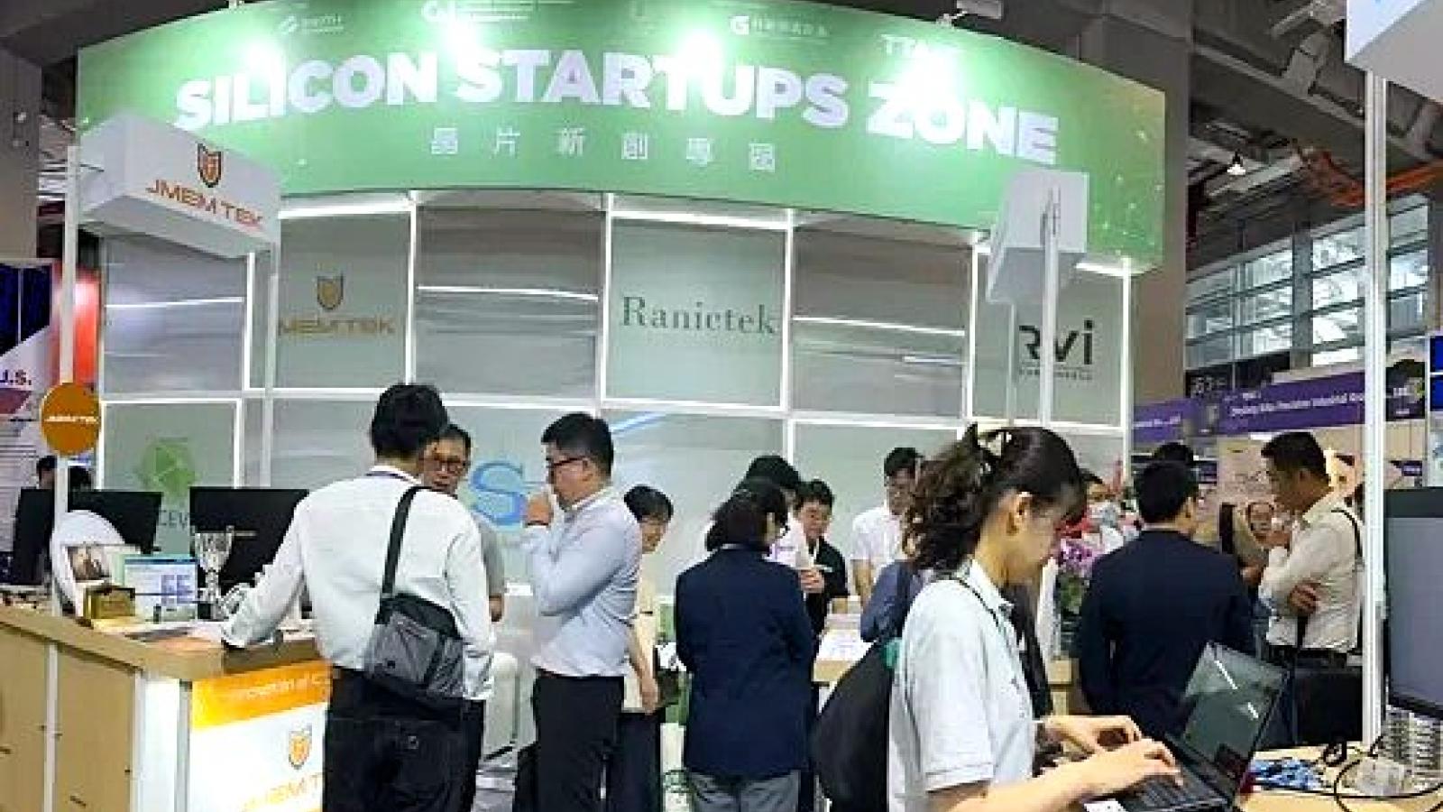
SEMICON Taiwan 2026 kicks off on August 31 with pre-show forums, followed by the physical exhibition running from September 2 to 4 at the Taipei Nangang Exhibition Center. The Silicon Startups Zone, hosted by SEMI, will be located on the 7th floor of Nangang Exhibition Hall 2, showcasing innovations across AI-driven systems, next-generation computing, quantum technologies, silicon photonics, advanced processes, advanced packaging, sustainable manufacturing, and semiconductor equipment and materials.
The number of teams in the startup showcase has increased from six last year to 16 this year—a more than doubling in scale. Technologies span advanced processes, AI computing, silicon photonics, semiconductor testing and metrology, smart manufacturing, and quantum computing. Innovation scope has also expanded from chip design tools to process development, advanced packaging, interconnect technologies, and system architecture.
Calvin Tsao, SEMI’s Global Marketing Officer and President of Taiwan, said AI is accelerating semiconductor technology evolution at an unprecedented pace, shortening innovation cycles. Companies that fail to grasp emerging technologies and R&D trends in real time risk missing the next wave of growth opportunities.
Tsao added that SEMI aims to connect semiconductor startups, industry leaders, investors, and manufacturing ecosystems through its global startup platform, helping enterprises identify breakthrough technologies earlier, speed up validation and collaboration, and keep pace with rapid innovation.
On the application of AI in semiconductor R&D, Leafy Lab will demonstrate how agentic AI and design automation can improve chip tape-out success rates. Unlike traditional generative AI, which produces content based on prompts, agentic AI can decompose tasks, plan workflows, and invoke different tools—potentially integrating deeply into electronic design automation (EDA) and chip development to reduce engineers’ time spent on complex designs.
As advanced chip design complexity and development costs continue to rise, unexpected tape-out results increase manufacturing costs and delay product launches. Therefore, whether AI can help engineering teams detect design flaws early, improve verification processes, and boost first-time tape-out success has become a key application area for agentic AI in the semiconductor industry.
Another startup, Nabu Optical Systems, targets chip prototyping by combining projection lithography with direct laser writing to develop a maskless direct-write lithography solution, aiming to lower prototype development costs and shorten process cycles. Japanese startup Elephantech uses nano-copper technology to advance high-density interconnects, through-glass vias (TGV), and next-generation advanced packaging applications—showcasing how semiconductor startups’ technological competition now extends from front-end chip design all the way to back-end packaging and heterogeneous integration.
Beyond agentic AI, overcoming data transmission and energy efficiency bottlenecks in AI systems is another key focus of this year’s startup stage. The three-day Silicon Startups Stage will host nearly 40 presentations across six themes: AI chip design and EDA, advanced manufacturing, advanced packaging and heterogeneous integration, silicon photonics and quantum technologies, next-generation AI computing architectures, and smart manufacturing, sustainability, and facility technologies.
Among them, Neurophos will develop high-speed, low-power AI inference using optical processors (OPUs) as the core. Ayar Labs will address large-scale AI systems’ data transfer and bandwidth demands through co-packaged optics (CPO) and optical input/output (I/O) technologies.
As GPU and AI accelerator clusters grow larger, system performance is no longer limited solely by individual chip compute power. High-speed data movement between chips and servers, along with the associated energy consumption during transmission, is becoming a bottleneck for scaling AI infrastructure. CPO tightly integrates optical components with compute or switch chips to shorten high-speed electrical signal transmission distances, alleviating bandwidth and power challenges faced by traditional electrical interconnects.
In quantum computing, Quantum Motion will present a silicon spin qubit architecture developed using standard CMOS processes. This approach leverages existing semiconductor manufacturing infrastructure to improve quantum chip scalability, seeking a viable path to move quantum computing from labs to mass production.
Whether technology can leave the lab depends on subsequent validation, customer adoption, and financial support. To fill a critical gap in semiconductor startup commercialization, SEMICON Taiwan is hosting its first Innovation Venture Day this year. Held on September 4 under an invitation-only format, it will connect semiconductor startups with corporate VCs, venture capital firms, and global ecosystem partners.
Morning sessions will feature speakers from Silicon Catalyst, Plug and Play, the Taiwan Stock Exchange, MediaTek Innovation Fund, UMC Capital, TEL Venture Capital, Samsung Ventures, and Lam Capital, sharing insights on semiconductor startup investment trends and practical experiences from perspectives such as startup incubation, corporate investment, and capital market development.
Notably, MediaTek Innovation Fund, UMC Capital, and Samsung Ventures have industrial ties to MediaTek, UMC, and Samsung respectively. TEL Venture Capital and Lam Capital are linked to semiconductor equipment makers Tokyo Electron and Lam Research. For semiconductor companies, investing in startups offers benefits beyond financial returns—including early access to cutting-edge technologies, complementing internal R&D, and building strategic partnerships.
An enterprise VC luncheon will gather members of SEMI’s High-Tech Innovation & Investment Committee, global corporate VCs, and ecosystem partners. In the afternoon, a startup pitch session will feature 10 to 12 high-potential startups selected by a committee of semiconductor industry experts, helping teams secure investment and strategic collaboration opportunities.
Compared to general software services, semiconductor startups face longer R&D cycles, higher tape-out and equipment costs, and complex customer validation procedures. Therefore, while SEMICON Taiwan’s expanded startup showcase and inaugural venture matchmaking are noteworthy, the true measure of success lies in whether interactions during the event translate into future process validation, supply chain collaborations, corporate investments, and actual orders.
FACT BOX
- Source: PR Times
- Category: Event
- Organizations: Leafy Lab / Nabu Optical Systems / Elephantech
- Products / services: Agentic AI