Even when breakthroughs in semiconductor new materials or new processes occur in university laboratories, they must undergo equipment adaptation, process integration, and mass production verification before being implemented in actual wafer fabs.
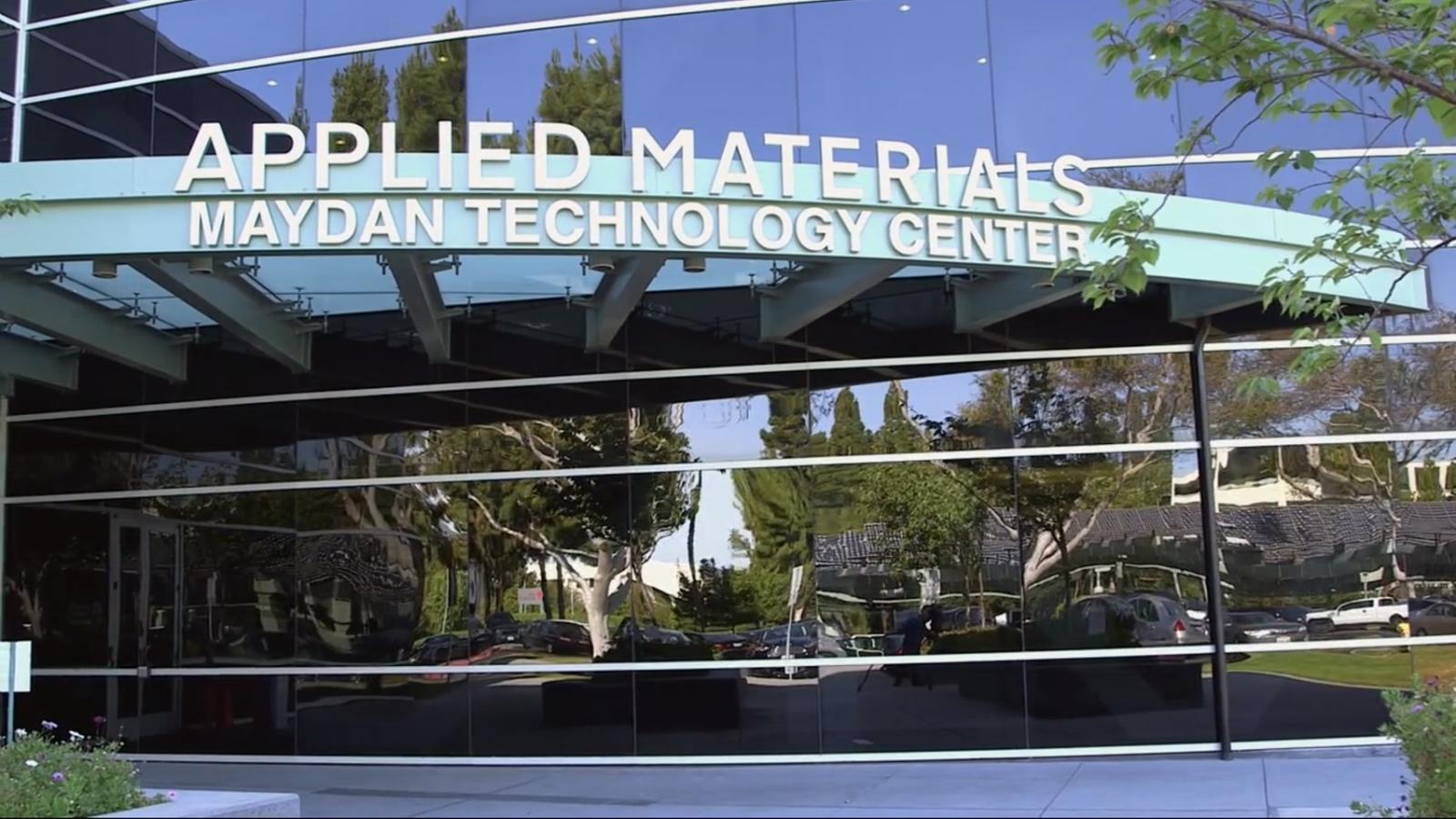
Applied Materials (NASDAQ: AMAT) announced that the University of California, Berkeley (UC Berkeley) will join its Silicon Valley-based Equipment and Process Innovation and Commercialization (EPIC) Center as a research partner. This enables academic researchers to access industry-grade chip manufacturing equipment, shortening the journey for AI chip materials and process technologies from the laboratory to mass production.
Under the collaboration plan, Berkeley research teams will jointly conduct research with Applied Materials scientists and engineers to advance materials engineering and process innovations required for AI computing. Compared to typical academic labs, the EPIC Center will provide equipment and process environments closer to the actual production needs of chip manufacturers, allowing researchers to accelerate technology iteration, process integration, and validation.
Applied Materials notes that research universities are often the birthplace of new material and process concepts. However, if research equipment, wafer sizes, and process conditions differ significantly from those in commercial wafer fabs,研究成果 may still require re-adjustment and re-validation when introduced into industrial settings. The EPIC Center aims to allow academia earlier access to the same equipment used by global chip manufacturers, thereby reducing the gap between academic research and industrial mass production.
Joint Industry-Academia Teams Share Industrial-Grade Equipment to Accelerate Commercialization
Prabu Raja, President of Applied Materials’ Semiconductor Products Group, said, "The EPIC Center is designed to bring together top talent from both industry and academia within a highly efficient R&D environment closely aligned with manufacturing needs, dramatically accelerating the development and commercialization of next-generation semiconductor technologies."
He added that few academic institutions have had as profound an impact on modern chip manufacturing as Berkeley. Applied Materials aims to expand its research collaboration through the EPIC Center, strengthen the pathway from lab to fab, and simultaneously build a platform for cultivating future semiconductor talent.
This partnership reflects a shift in semiconductor R&D models. In the past, academia, equipment vendors, and chipmakers typically took turns advancing technology development. But as AI chips evolve toward 3D structures, heterogeneous integration, and new materials, the interactions among materials, equipment, and processes have become increasingly complex. If each stage is developed separately, repeated corrections may be needed during mass production validation, prolonging the time to commercialization.
The model adopted by the EPIC Center brings academic research teams, equipment suppliers, and industry partners into a shared R&D environment earlier, validating new materials and processes on industrial-grade equipment. Its core goal is not to replace fundamental university research, but to add an integration and validation platform between academic achievements and mass production in wafer fabs.
From SPICE and FinFET to AI Chips: Continuing Berkeley’s Research Legacy
Berkeley has long been committed to fundamental semiconductor research and technology transfer. The university established a dedicated research lab for integrated circuit prototyping in 1962. Subsequent landmark achievements include the SPICE circuit simulator and FinFET (Fin Field-Effect Transistor), which became foundational to advanced logic processes worldwide.
SPICE allows chip designers to simulate circuit behavior via software, while FinFET improves gate control and reduces leakage current through a three-dimensional transistor structure. These two technologies have had long-term impacts on the modern semiconductor industry—SPICE at the design tool level and FinFET at the transistor architecture level.
Applied Materials believes that Berkeley’s accumulated experience in research and technology transfer aligns perfectly with the EPIC Center’s mission to accelerate the adoption of new technologies into industry. However, SPICE and FinFET represent Berkeley’s past landmark achievements and are not new outcomes of the current EPIC collaboration.
Mark Asta, Dean of the College of Engineering at Berkeley, stated that innovative contributions from Berkeley researchers have driven advancements in chip technology, enhanced computing power, and helped usher in the AI era. The EPIC Center established by Applied Materials will enable research universities to access the latest, industry-synchronized semiconductor process equipment and technologies earlier, accelerating the transformation of research results into commercial applications.
EPIC Center to Launch in 2026, Strengthening Silicon Valley’s Innovation Ecosystem
EPIC stands for Equipment and Process Innovation and Commercialization. According to Applied Materials’ plans, the center will be located in Silicon Valley and begin operations in 2026. Its primary mission is to shorten the commercialization timeline for breakthrough technologies from early research to full-scale mass production.
Applied Materials describes the EPIC Center as the largest investment to date in advanced semiconductor equipment R&D in the United States. However, this press release does not disclose specific investment amounts, initial research projects, or technology adoption timelines.
The collaboration between Berkeley and Applied Materials is not starting from scratch. The two parties have previously established cooperative relationships through semiconductor research programs and shared laboratory resources, including initiatives under the Berkeley Emerging Technologies Research (BETR) center and the Center for Information Technology Research in the Interest of Society (CITRIS).
Moreover, many Berkeley alumni currently serve as engineers, scientists, and managers at Applied Materials, and the company continues to recruit talent annually from the university. Both organizations being based in Silicon Valley facilitates the seamless flow of research ideas, engineering talent, and equipment resources between campus and industry.
As AI chips incorporate more new materials, 3D structures, and heterogeneous integration technologies, the pace of semiconductor innovation depends not only on who proposes the initial research idea first, but also on how quickly equipment validation, process integration, and mass production ramp-up can be completed. With Berkeley joining the EPIC Center, whether this industry-academia co-development model can truly shorten the time for new technologies to move from the lab to the fab will be a key point of observation going forward.
FACT BOX
- Source: PR Times
- Category: Partnership
- Organizations: Applied Materials / UC Berkeley