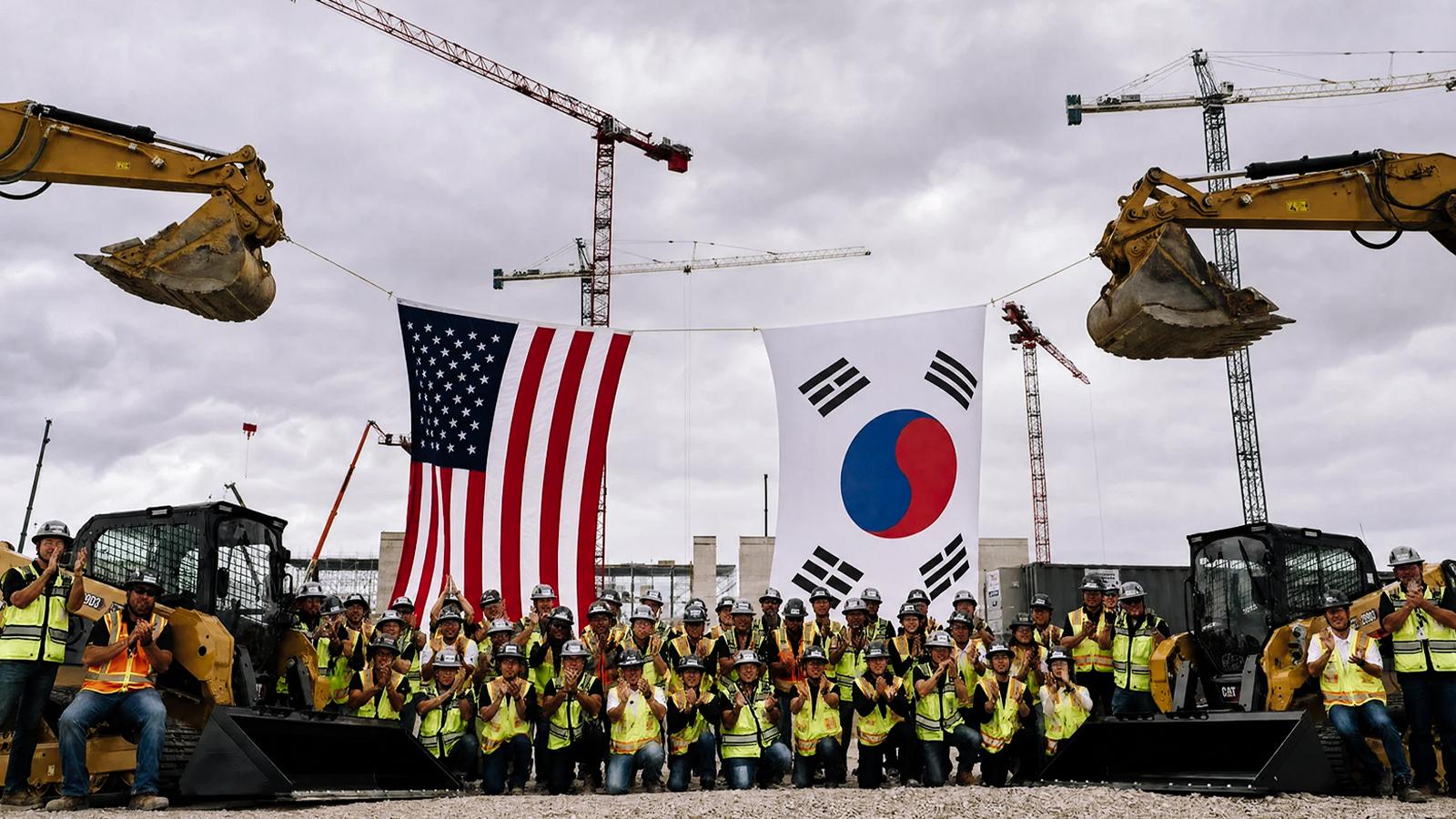
South Korea's memory giant SK Hynix, one of the biggest winners amid the artificial intelligence (AI) boom, is not only strengthening its domestic manufacturing but also expanding its footprint in the United States. CEO Kwak Noh-Jung recently announced that the company's new facility in Indiana will, by 2030, transform the state into the core hub for high-bandwidth memory (HBM) production in the U.S., aligning with the Trump administration's 'Made in America' vision.
SK Hynix held a grand groundbreaking ceremony in West Lafayette, Indiana, for its first U.S. facility. In his speech, the CEO emphasized the urgent market demand for HBM driven by the global AI surge, stating, 'We will provide our customers with a new source of HBM made in the U.S., while strengthening the security and development of America’s semiconductor supply chain.'
U.S. Investment to Exceed $45 Billion by 2030
According to CNBC, SK Hynix, the global leader in HBM market share, is undertaking a massive $720 billion (approximately NT$23.04 trillion) expansion, with the majority of capacity concentrated in its largest memory chip campus under construction in South Korea. If progress remains on track, the campus is expected to begin operations in February 2027.
Meanwhile, the $4 billion (approximately NT$128 billion) Indiana facility will focus on 'advanced packaging' rather than front-end wafer fabrication. In other words, memory chips manufactured in South Korea and China will be shipped to the U.S. for stacking and interconnection.
SK Hynix stated that the first cleanroom for packaging operations is expected to be officially operational by October 2028. Including prior investments such as its AI-focused subsidiary and the acquisition of Intel’s NAND business, the company’s total U.S. investment and asset scale will exceed $45 billion (approximately NT$1.44 trillion) by 2030.
U.S. Commerce Secretary Remains Unimpressed
Although advanced packaging is a critical back-end process in chip manufacturing, U.S. Commerce Secretary Howard Lutnick expressed dissatisfaction in July, publicly urging SK Hynix and its main rival Samsung Electronics to build front-end 'wafer fabrication plants' directly on U.S. soil.
In response to this criticism, SK Hynix’s CEO told international media that the company is actively seeking suitable opportunities and remains open to any location or country, pledging to continue expanding its U.S. investments and collaboration.
Indiana’s Republican Governor Mike Braun hailed the project as the largest development in the state’s history and a major milestone for the entire nation. Senator Todd Young noted, 'For too long, the U.S. has designed advanced chips while allowing the manufacturing ecosystem to drift overseas. Today’s groundbreaking is the best evidence that supply chains are returning.'
Collaborating with NVIDIA and Purdue University to Build an AI Memory Ecosystem
Official data from Indiana reveals that the project will receive up to $458 million (approximately NT$14.65 billion) in federal CHIPS Act subsidies and $712 million (approximately NT$22.78 billion) in state incentives—the second-largest in state history. Across the 133-acre production campus, in addition to the advanced packaging plant, a research and development center will be established to enable top-tier AI customers to co-develop next-generation memory solutions.
Notably, NVIDIA, the leader in AI chips, has committed to co-developing memory with SK Hynix as part of a $500 billion (approximately NT$16 trillion) partnership signed in July.
In terms of future workforce and job creation, the Indiana plant is expected to generate around 1,000 direct jobs and over 6,000 indirect jobs. Initially, SK Hynix will dispatch personnel from South Korea, but once operations stabilize, the company plans to hire extensively from Purdue University’s semiconductor talent pool, building an industry-academia integrated AI memory ecosystem.
FACT BOX
- Source: PR Times
- Category: Event